Recently, Xuejin Zhang’s research group in the College of Engineering and Applied Sciences at Nanjing University have made significant progress in the field of ultra-compact photodetection. By combining a 2D transition metal dichalcogenides (TMDCs) with a well-designed plasmonic metasurface, they extend the photoelectric response range from the visible to near-infrared second (NIR-II) window, make the sensitivity comparable to those of commercial NIR-II detectors, and realize chiral discrimination. This work breaks the bottleneck of 2D material photodetectors, paving the way for practical applications such as biomedical imaging, molecular chirality characterization, fiber-optic communications, and on-chip spectrometer development. The results were published in Nature Communications (Nat. Commun.17, 2907 (2026)), titled as “Anapole-state-enhanced 2D chiral photodetector operating in the near-infrared second window”.
Research Background
2D TMDCs are regarded as ideal candidate materials for next-generation optoelectronic devices due to their atomic thickness, strong excitonic effects, and excellent mechanical flexibility. However, conventional 2D material photodetectors are constrained by their intrinsic bandgaps, with response bands primarily concentrated in the visible range, making it difficult to cover the NIR-II window—a spectral region crucial for biomedical imaging and fiber-optic communications. Although nonlinear optical processes such as two-photon absorption can broaden the response band, their intrinsic efficiency is extremely low, severely restricting practical applications.
Breaking Wavelength Limit of 2D Material Detection via Optical Field Manipulation
How to overcome above challenge? Leveraging their prior expertise and deep understanding of light–matter interactions, the research group proposed a solution: on-chip integration of high-quality single-crystalline Ag plasmonic metasurfaces with MoS2/WSe2 van der Waals heterostructures.
The core of this scheme lies in:
Constructing Higher-Order Multipoles: Loss-controlled quasi-bound states in the continuum (quasi-BICs) are utilized, and higher-order multipoles are awakened via anapole states. Under this circumstance, electromagnetic field is tightly confined in space. A local electric field enhancement exceeding 800-fold can then be achieved, providing unprecedented augmentation for nonlinear optical processes such as two-photon absorption.
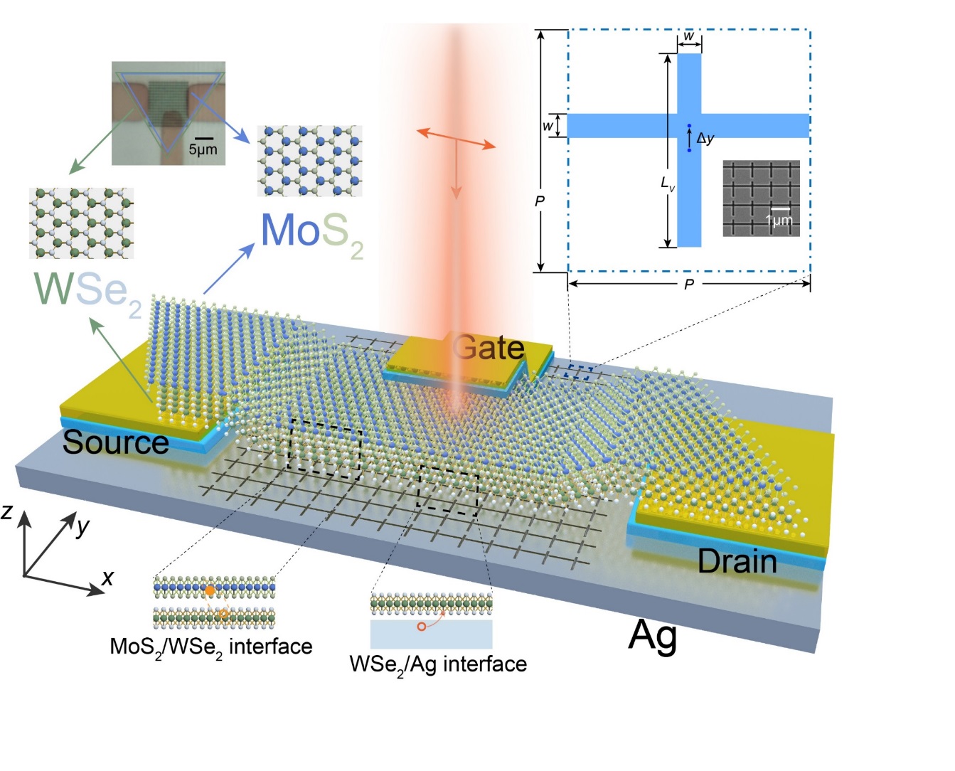
Figure 1. Schematic illustration of the high-performance photodetector.
Synergizing Multiple Enhancement Mechanisms: The photoresponse of the device arises from three contributions: enhanced two-photon absorption, hot carrier injection from plasmon relaxation, and resonant enhancement of interlayer excitons in the heterostructure. This synergy between optical and electrical processes results in a device performance improvement of approximately 50,000 times compared to unstructured devices. The device achieves a responsivity of 1.35 A/W at 1550 nm, rivaling commercial InGaAs detectors.
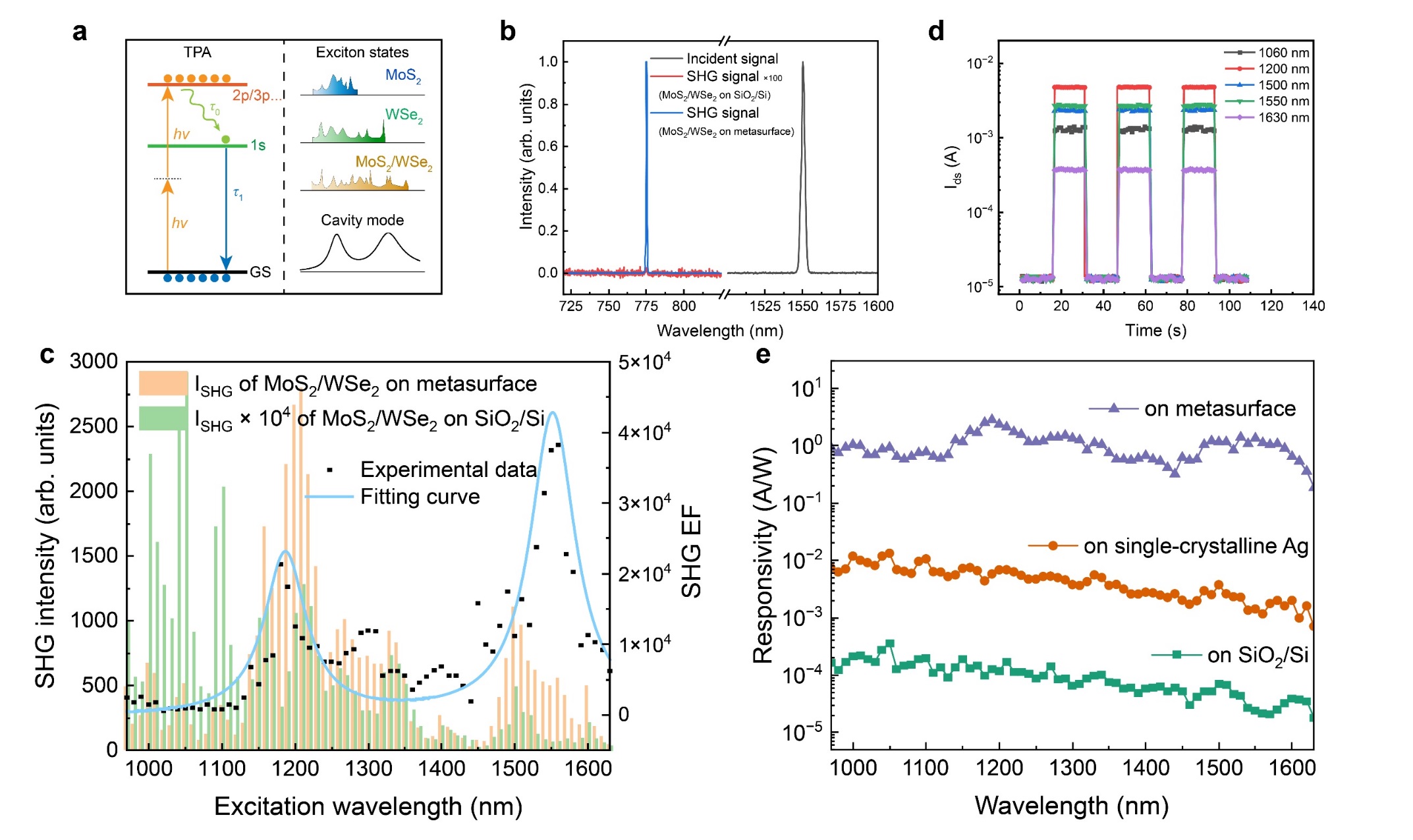
Figure 2. Optical and optoelectronic enhancement of the device. a, Left: Schematic of two-photon absorption process under exciton resonance. Right: Resonance modes of the device. b, Normalized spectra of the fundamental laser (right, 1550 nm) and SHG signal (left, 775 nm) generated from the MoS2/WSe2 heterostructure on SiO2/Si substrate (magnified 100-fold) and on Ag metasurface. SHG: second harmonic generation. c, Measured SHG intensity of the MoS2/WSe2 heterostructure on SiO2/Si and Ag metasurface under excitation wavelengths from 975 to 1625 nm. The signal intensity on SiO2/Si substrate has been magnified 104-fold. Right axis: SHG enhancement factor calculated from experimental data. d, On/off switching behavior of the MoS2/WSe2 heterostructure on Ag metasurface under 2 mW laser excitation. e, Photoresponse of the MoS2/WSe2 heterostructure on Ag metasurface, single-crystalline Ag, and SiO2/Si substrates in the NIR-II window.
This study systematically elucidates the critical role of higher-order multipoles in enhancing the nonlinear optical processes of 2D materials. Using asymmetric structure arrays on single-crystalline Ag surfaces, the research group precisely controlled over local optical field. Numerical simulations and experimental results indicate that the quasi-BICs supported by this metasurface are predominantly governed by higher-order multipoles such as electric quadrupole. Unlike conventional electric dipole, these higher-order multipoles exhibit significantly smaller effective mode volumes and stronger near-field confinement.
Multifunctional Integrated Optoelectronic Response
In experimental validation, the research group further demonstrated the device’s linear and circular polarization resolution capabilities in optical and optoelectronic responses:
Linear Polarization Resolution: Due to the differential response of the structure to light of different linear polarizations, the photocurrent exhibits strong anisotropy, achieving a linear polarization ratio as high as 40—far exceeding that of conventional 2D material photodetectors.
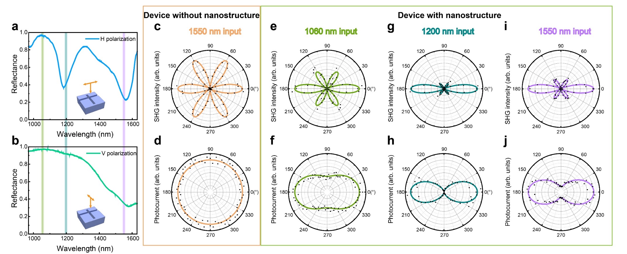
Figure 3. Linear polarization characteristics of the device. a,b, Measured reflectance spectra of the hybrid structure under horizontally (a) and vertically (b) polarized incident light. The three colored shaded areas represent the wavelengths measured in c–j: 1060 nm, 1200 nm, and 1550 nm. c,d, Polar plots of the normalized perpendicular component of SHG intensity (c) and photocurrent (d) from the MoS2/WSe2 heterostructure on SiO2/Si substrate under 1550 nm illumination, with the sample rotated 360°. e–j, Polar plots of the normalized perpendicular component of SHG intensity (e,g,i) and photocurrent (f,h,j) from the MoS2/WSe2 heterostructure on the metasurface under 1060 nm (e,f), 1200 nm (g,h), and 1550 nm (i,j) illumination, with the sample rotated 360°.
Chiral Resolution: By introducing a mirror asymmetry of the metasurface, the device shows distinctly different absorption and photocurrent responses to left-handed and right-handed circularly polarized light. The circular polarization photocurrent discrimination ratio reaches 7.2 at 1550 nm and can be tuned by adjusting structural parameters, promising a new generation of compact chiral spectroscopic analysis devices.
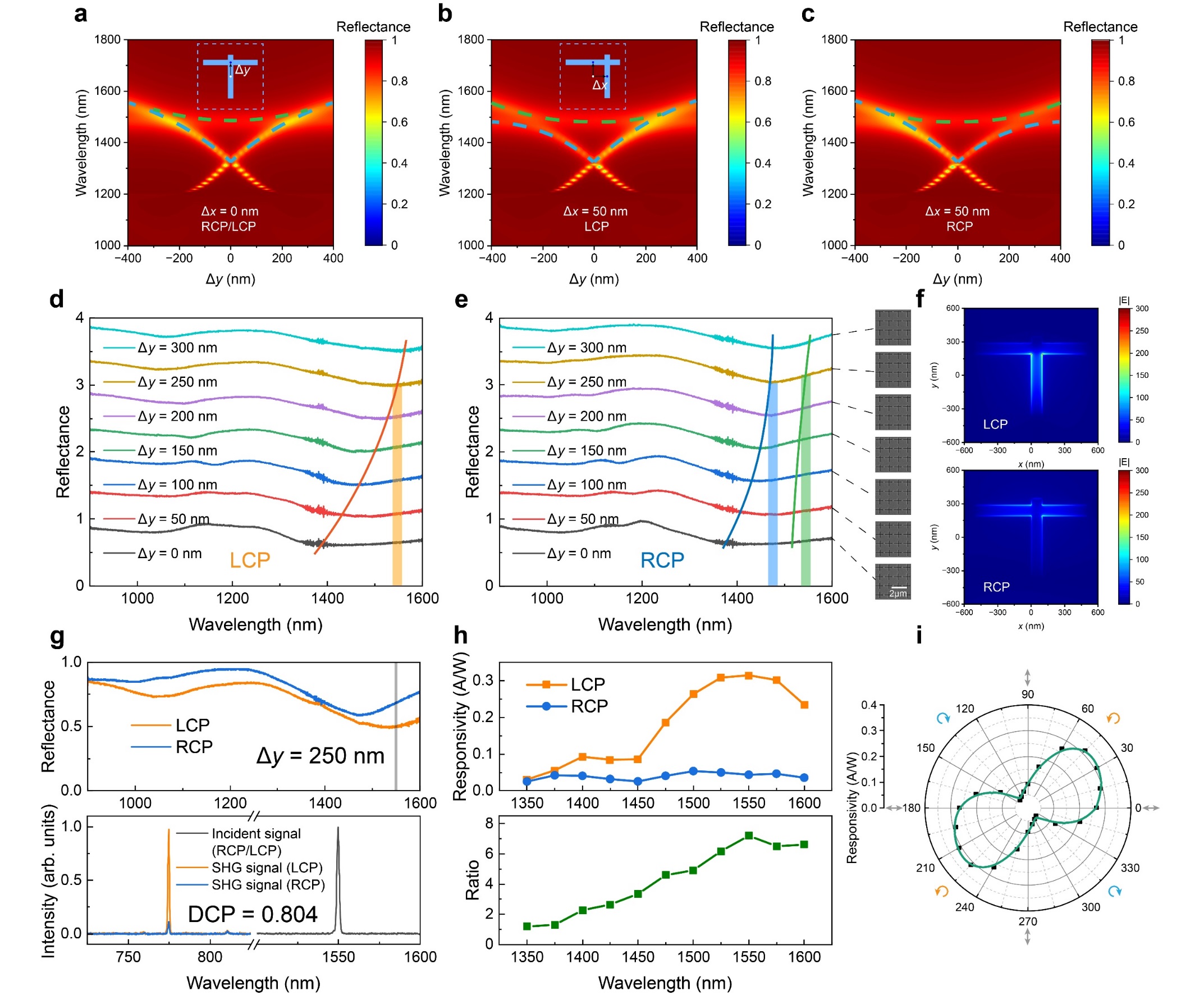
Figure 4. Chiral optoelectronic response of the device. a, Calculated mapping of reflectance spectra under left-handed circularly polarized (LCP) and right-handed circularly polarized (RCP) illumination as a function of structural asymmetry Δy. The period is increased to P = 1200 nm compared to the structure in Figure 1. b,c, Calculated mapping of reflectance spectra under LCP (b) and RCP (c) illumination as a function of Δy, with mirror symmetry broken by Δx = 50 nm. d,e, Measured reflectance spectra under LCP (d) and RCP (e) illumination as a function of Δy, with Δx = 50 nm. SEM images are shown alongside. f, Calculated electric field intensity distributions on the metasurface unit cell under LCP and RCP illumination at a wavelength of 1550 nm, with Δx = 50 nm and Δy = 250 nm. g, Top: Measured reflectance spectra under LCP and RCP illumination at Δx = 50 nm and Δy = 250 nm. Bottom: Normalized spectra of the fundamental laser (right, 1550 nm) and SHG signal (left, 775 nm) generated from the MoS2/WSe2 heterostructure on the Ag metasurface under LCP (orange) and RCP (blue) illumination. h, Top: Responsivity spectra under LCP and RCP illumination. Bottom: Chiral discrimination ratio of the optoelectronic response. i, Polar diagram of responsivity as a function of ellipticity angle at a wavelength of 1550 nm.
Applications and Future Perspectives
The photodetector developed on this platform successfully demonstrates the immense potential of nanophotonic engineering to overcome the intrinsic limitations of 2D materials. In the future, this technology is expected to play a key role in the following areas:
NIR-II Biomedical Imaging: High sensitivity in the NIR-II window supports high-resolution in vivo imaging of deep tissues.
High-Speed Fiber-Optic Communications: As a core receiving-end device compatible with existing communication bands, its room-temperature operation simplifies system design and reduces power consumption.
Multifunctional Integrated Optoelectronic Chips: The spectral detection capability can also be built in this platform by means of structural design, enabling compact, multi-dimensional (intensity, wavelength, polarization) optical information detection on a single chip.
Flexible and Wearable Optoelectronic Systems: Combined with the flexibility of 2D materials, this enhancement strategy provides technical support for the development of high-performance, bendable portable sensing devices.
In summary, this study not only demonstrates a general method for dramatically enhancing the nonlinear optical conversion efficiency of 2D materials through anapole states and quasi-BICs, but also endows the device with chiral detection capabilities through structural symmetry design. It offers an innovative paradigm for next-generation high-performance, multifunctional on-chip integrated optoelectronic devices.
The research was supported by the National Key R&D Program of China, the National Natural Science Foundation of China, and the Natural Science Foundation of Jiangsu Province.
Article link: https://doi.org/10.1038/s41467-026-69727-z